- 您现在的位置:买卖IC网 > Sheet目录985 > ISL29010IROZ-EVALZ (Intersil)EVALUATION BOARD FOR ISL29010
�� �
�
�ISL29010�
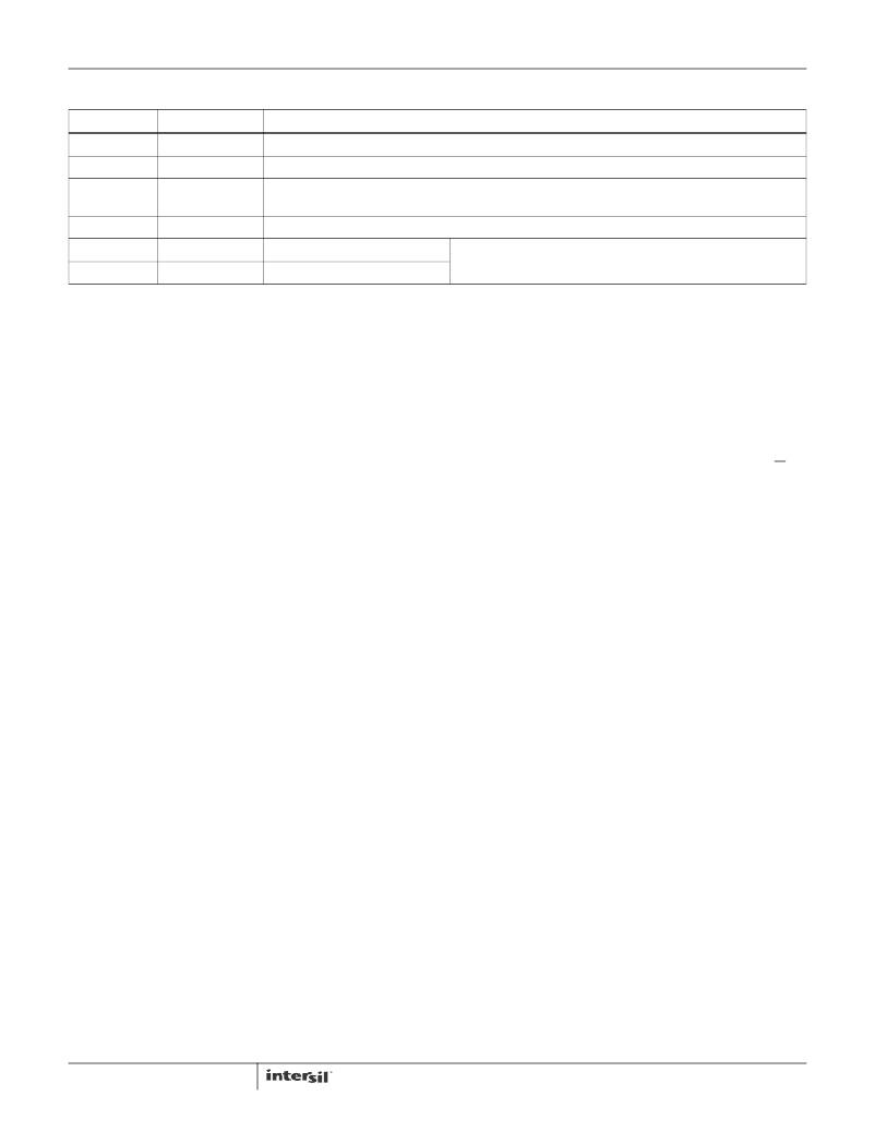
�Pin� Descriptions�
�PIN� NUMBER�
�1�
�2�
�3�
�4�
�PIN� NAME�
�VDD�
�GND�
�REXT�
�A0�
�DESCRIPTION�
�Positive� supply;� connect� this� pin� to� a� regulated� 2.5V� to� 3.3V� supply�
�Ground� pin.� The� thermal� pad� is� connected� to� the� GND� pin�
�External� resistor� pin� for� ADC� reference;� connect� this� pin� to� ground� through� a� (nominal)� 100k� Ω� resistor� with�
�1%� tolerance�
�Bit� 0� of� I� 2� C� address�
�5�
�6�
�SCL�
�SDA�
�I� 2� C� serial� clock�
�I� 2� C� serial� data�
�The� I� 2� C� bus� lines� can� pulled� above� VDD,� 5.5V� max.�
�Principles� of� Operation�
�Photodiodes�
�The� ISL29010� contains� two� photodiode� arrays� which� convert�
�light� into� current.� Some� diodes� are� sensitive� to� both� visible�
�and� infrared� light,� while� the� others� are� only� sensitive� to�
�infrared� light.� Using� the� infrared� portion� of� the� light� as�
�baseline,� the� visible� light� can� be� extracted.� The� spectral�
�response� vs� wavelength� is� shown� in� Figure� 6� in� the� “Typical�
�Performance� Curves”� on� page� 9.� After� light� is� converted� to�
�current� during� the� light� data� process,� the� current� output� is�
�converted� to� digital� by� a� single� built-in� integrating� type� signed�
�15-bit� Analog-to-Digital� Converter� (ADC).� An� I� 2� C� command�
�reads� the� visible� light� intensity� in� counts.�
�The� converter� is� a� charge-balancing� integrating� type� signed�
�15-bit� ADC.� The� chosen� method� for� conversion� is� best� for�
�converting� small� current� signals� in� the� presence� of� an� AC�
�periodic� noise.� A� 100ms� integration� time,� for� instance,� highly�
�rejects� 50Hz� and� 60Hz� power� line� noise� simultaneously.� See�
���The� built-in� ADC� offers� user� flexibility� in� integration� time� or�
�conversion� time.� There� are� two� timing� modes:� Internal� Timing�
�Mode� and� External� Timing� Mode.� In� Internal� Timing� Mode,�
�integration� time� is� determined� by� an� internal� dual� speed�
�oscillator� (f� OSC� ),� and� the� n-bit� (n� =� 4,� 8,� 12,� 16)� counter� inside�
�the� ADC.� In� External� Timing� Mode,� integration� time� is�
�determined� by� the� time� between� two� consecutive� I� 2� C� External�
�Timing� Mode� commands.� See� External� Timing� Mode� example.�
�A� good� balancing� act� of� integration� time� and� resolution�
�(depending� on� the� application)� is� required� for� optimal� results.�
�The� ADC� has� four� I� 2� C� programmable� range� select� to�
�dynamically� accommodate� various� lighting� conditions.� For�
�very� dim� conditions,� the� ADC� can� be� configured� at� its� lowest�
�range.� For� very� bright� conditions,� the� ADC� can� be� configured�
�at� its� highest� range.�
�I� 2� C� Interface�
�There� are� eight� (8)� 8-bit� registers� available� inside� the� ISL29010.�
�The� command� and� control� registers� define� the� operation� of� the�
�device.� The� command� and� control� registers� do� not� change� until�
�the� registers� are� overwritten.� There� are� two� 8-bit� registers� that�
�3�
�set� the� high� and� low� interrupt� thresholds.� There� are� four� 8-bit�
�data� Read� Only� registers,� two� bytes� for� the� sensor� reading� and�
�another� two� bytes� for� the� timer� counts.� The� data� registers�
�contain� the� ADC's� latest� digital� output,� and� the� number� of� clock�
�cycles� in� the� previous� integration� period.�
�The� ISL29010� has� a� 7-bit� I� 2� C� interface� slave� address.� The�
�six� most� significant� bits� are� hardwired� internally� as� 100010�
�while� the� least� significant� bit� A0� can� be� either� connected� to�
�Ground� or� VDD� to� allow� two� possible� addresses� 1000100� or�
�1000101.� When� 1000100x� or� 1000101x� with� x� as� R� or� W� is�
�sent� after� the� Start� condition,� this� device� compares� the� first�
�seven� bits� of� this� byte� to� its� address� and� matches.�
�Figure� 1� shows� a� sample� one-byte� read.� Figure� 2� shows� a�
�sample� one-byte� write.� Figure� 3� shows� a� sync_I� 2� C� timing�
�diagram� sample� for� externally� controlled� integration� time.�
�The� I� 2� C� bus� master� always� drives� the� SCL� (clock)� line,� while�
�either� the� master� or� the� slave� can� drive� the� SDA� (data)� line.�
�Figure� 2� shows� a� sample� write.� Every� I� 2� C� transaction� begins�
�with� the� master� asserting� a� start� condition� (SDA� falling� while�
�SCL� remains� high).� The� following� byte� is� driven� by� the�
�master,� and� includes� the� slave� address� and� read/write� bit.�
�The� receiving� device� is� responsible� for� pulling� SDA� low�
�during� the� acknowledgement� period.�
�Every� I� 2� C� transaction� ends� with� the� master� asserting� a� stop�
�condition� (SDA� rising� while� SCL� remains� high).�
�For� more� information� about� the� I� 2� C� standard,� please� consult�
�the� Philips� ?� I� 2� C� specification� documents.�
�FN6414.1�
�November� 11,� 2011�
�发布紧急采购,3分钟左右您将得到回复。
相关PDF资料
ISL29011IROZ-EVALZ
EVAL BOARD FOR ISL29011
ISL29012IROZ-EVALZ
EVALUATION BOARD ISL29012IROZ
ISL29013IROZ-EVALZ
EVALUATION BOARD FOR ISL29013
ISL29015IROZ-EVALZ
EVALUATION BOARD FOR ISL29015
ISL29018IROZ-EVALZ
EVALUATION BOARD FOR ISL29018
ISL29020IROZ-EVALZ
EVALUATION BOARD FOR ISL29020
ISL29021IROZ-EVALZ
EVAL BOARD FOR ISL29021IROZ
ISL29023IROZ-EVALZ
EVALUATION BOARD ISL29023IROZ
相关代理商/技术参数
ISL29010IROZ-T7
功能描述:光学数位转换器 ISL29010IROZ LIGHT TO-DIGTL OUTPUT SENS RoHS:否 制造商:ams 数据总线宽度: 峰值波长:470 nm 最大工作频率: 工作电源电压: 工作电流: 最大工作温度:+ 85 C 最小工作温度:- 40 C 封装 / 箱体:Chipscale-6 封装:Reel
ISL29011IROZ-EVALZ
功能描述:EVAL BOARD FOR ISL29011 RoHS:是 类别:编程器,开发系统 >> 评估板 - 传感器 系列:* 产品培训模块:Lead (SnPb) Finish for COTS
Obsolescence Mitigation Program 标准包装:1 系列:-
ISL29011IROZ-T7
功能描述:IC PROXIMITY SENSOR AMB LT 8ODFN RoHS:是 类别:传感器,转换器 >> 多功能 系列:- 其它有关文件:Automotive Product Guide 标准包装:2,500 系列:- 传感器类型:光线和近程 输出类型:I²C?
ISL29011IROZ-T7R5484
制造商:Intersil Corporation 功能描述:ISL29011IROZ-T7 DOMINANT ASSY AND UNISEM TEST ONLY - Tape and Reel 制造商:Intersil Corporation 功能描述:IC PROXIMITY SENSOR AMB LT 8ODFN 制造商:Intersil Corporation 功能描述:ISL29011IROZ-T7 DOMINANT ASSY AND CARSEM TEST ONLY T/R
ISL29012IROZ-EVALZ
功能描述:EVALUATION BOARD ISL29012IROZ RoHS:是 类别:编程器,开发系统 >> 评估板 - 传感器 系列:- 产品培训模块:Lead (SnPb) Finish for COTS
Obsolescence Mitigation Program 标准包装:1 系列:-
ISL29012IROZ-T7
功能描述:IC SENSOR LIGHT-DGTL I2C 6-ODFN RoHS:是 类别:传感器,转换器 >> 光学 - 光电探测器 - 环境光传感器 系列:- 产品培训模块:Lead (SnPb) Finish for COTS
Obsolescence Mitigation Program 产品变化通告:Product Discontinuation 25/Jun/2012 标准包装:2,500 系列:- 带接近传感器:无 波长:- 电源电压:1.7 V ~ 2 V 电流 - 暗(标准):- 电流 - 光(典型值):- 输出类型:数字 - I²C 工作温度:-40°C ~ 85°C 安装类型:表面贴装 封装/外壳:6-UDFN 裸露焊盘 包装:带卷 (TR)
ISL29013IROZ
制造商:Intersil Corporation 功能描述:Light-To-Digital Sens,ISL29013IROZ
ISL29013IROZ-EVALZ
功能描述:EVALUATION BOARD FOR ISL29013 RoHS:是 类别:编程器,开发系统 >> 评估板 - 传感器 系列:- 产品培训模块:Lead (SnPb) Finish for COTS
Obsolescence Mitigation Program 标准包装:1 系列:-